CONCEPT
Home
 モチベーション
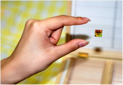
弊社のモチベーションは、非破壊、無電源、非接触、外部信号が必要ない解析法の研究開発です。例えば、プレパラートにのせた半導体チップをサンプルBOXから取り出し、顕微鏡で見るような感覚で電気的な故障解析が簡便にできる手法の提案です。
Non bias. Non contact. Non external signal. As for our method, the fault analysis can be carried out by a simple process of watching the semiconductor chip put on a preparation with a light microscope. The power supply, signal and electric wiring to be connected are not necessary.
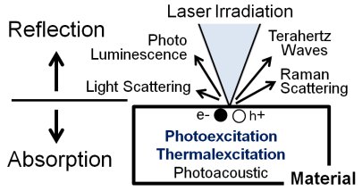
非接触を実現する物理現象
弊社のセンサはレーザ光を材料に照射して変化する電荷を検出して微小領域の電界(帯電状態)を検出します。
The figure indicates a physical phenomenon by laser irradiation.Signal
from the material is largely categorized as reflection and absorption.
We focused on photo excitation and thermal excitation which diffuse in
the material.
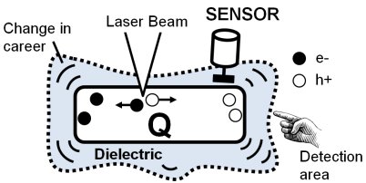
微小領域の電界検出
弊社は材料付近に存在する準静電界(QEF:Qasi Electostatic Field)を利用します。
This chart, QEF is where charged carriers change periodically.Such changing
carriers are detected by using SENSOR.Therefore, the charge amount Q for
object follows the unchanged rule.Quasi-electrostatic field is distributed
in the vicinity of the object and can be detected anywhere if it is located
near.
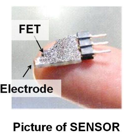
弊社の微小領域センサー
センサーの原理試作品の外観です。入力ゲート容量が小さいFETと低ノイズアンプを組み合わせ、モジュール化しています。
センサのサンプルを提供しています。一般サンプル価格: 80,000円 アカデミック価格:25,000円(税別)。使用に際しては、接続ケーブルと専用アンプが必要です。詳しくは、別途お問い合わせください。
The fundamental principle utilizes an electrostatic induction to a gate of FET. The change of gate voltage will be detected by conversion of a larger change of Drain current.The detection electrode is directly connected with gate of FET. The FET is high mobility depression type and input gate is zero-volt biased.Noise from outside have to be suppressed as much as possible, therefore sample and SENSOR is covered by shield.
Home
(c) 2012 Konaka Electronics, All Rights Reserved.